


Electronic pcb assembly, pcba board, circuit board for sale
Other recommendations for your business


Contact us
Quik Detail
| Model Number | Customized |
|---|---|
| Type | consumer electronics pcba |
| Place of Origin | Guangdong, China |
| Brand Name | UC |
| Supplier Type | OEM |
| Copper Thickness | 1oz |
| Metrials | FR-4,Aluminum,CEM-1 etc |
| Certificate | CE,ROHS,SGS etc |
| OEM/ODM | Support |
| MOQ | 1 PC |
| Copper thickness | 0.25OZ~12OZ |
| Min. Hole Size | 0.01mm |
| Min. Line Spacing | 0.01mm |
| Min. Line Width | 0.01mm |
| Base Material | FR4 |
Product Detail
PCB PCBA OEM Electronic Manufacturer Service
U-C Group Limited is an Electronic PCB & PCBA manufacturer.


PCB Technical Capacity
Layers | Mass production: 2~58 layers / Pilot run: 64 layers |
Max. Thickness | Mass production: 394mil (10mm) / Pilot run: 17.5mm |
Material | FR-4 (Standard FR4, Mid-Tg FR4,Hi-Tg FR4, Lead free assembly material) , Halogen-Free, Ceramic filled , Teflon, Polyimide, BT, PPO, PPE, Hybrid, Partial hybrid, etc. |
Min. Width/Spacing | Inner layer: 3mil/3mil (HOZ), Outer layer: 4mil/4mil(1OZ) |
Max. Copper Thickness | UL certificated: 6.0 OZ / Pilot run: 12OZ |
Min. Hole Size | Mechanical drill: 8mil(0.2mm) Laser drill: 3mil(0.075mm) |
Max. Panel Size | 1150mm × 560mm |
Inner layer: 3mil/3mil(HOZ), Outer layer: 4mil/4mil (1OZ) | Inner layer: 3mil/3mil (HOZ), Outer layer: 4mil/4mil(1OZ) |
Aspect Ratio | 18:1 |
Surface Finish | UL certificated: 6.0 OZ / Pilot run: 12OZ |
Special Process | Buried Hole, Blind Hole, Embedded Resistance, Embedded Capacity, Hybrid, Partial hybrid, Partial high density, Back drilling, and Resistance control. |
PCBA Technical Capacity
SMT | Position accuracy:20 um Components size:0.4×0.2mm(01005) -130×79mm,Flip-CHIP,QFP,BGA,POP Max. component height:25mm Max. PCB size:680×500mm Min. PCB size:no limited PCB thickness:0.3 to 6mm PCB weight:3KG |
Wave-Solder | Max. PCB width:450mm Min. PCB width: no limited Component height:Top 120mm/Bot 15mm |
Sweat-Solder | Metal type :part, whole, inlay, sidestep Metal material:Copper , Aluminum Surface Finish:plating Au, plating sliver , plating Sn Air bladder rate:less than20% |
Press-fit | Press range:0-50KN Max. PCB size:800X600mm |
Testing | ICT,Probe flying,burn-in,function test,temperature cycling |
IoT PCBA
HDI PCBA
Rigid-Flex PCB


Cooperation Customer


PCB Workshop


PCBA Workshop


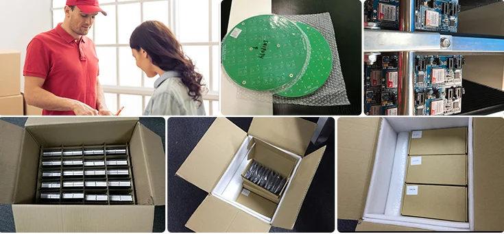
Each products with ESD bags (or on your request).
Provide the hard outer packing carton, to protect the goods during transport.
Transport:
Sample: 2~3 weeks by DHL,UPS,FedEx etc.
Order: 3~4 weeks (depend on the quantity of order)
The best shipping cost we can get from professional shipping company if with long-term cooperation.

Paypal, Western Union,T/T, Alipay, Secure Payment in Alibaba.

Q: Are you manufacturer?
A: Yes we are manufacturer.
Q: Do you provide samples?
A: Yes we can provide free samples, price and shipping cost open for negotiation.
Q: What certificates does this product have?
A: We have CE, FCC, ROHS certified.
Q: What about OEM and ODM?
A: We accept OEM and ODM orders, MOQ is open for discussion.
Q: What is depvery terms and time?
A: We use FOB terms and ship the goods in 7-30 days depend on your order quantity, customization.